
Research
This section intends to present superficially the main activities, those developed and under development.
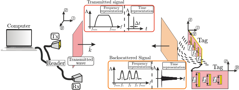
Chipless RFID tags
The chipless RFID technology is inscribed as an intermediate technology between the barcode and
the UHF-RFID [1]. The chipless RFID
incorporates
some of the
barcode's and UHF-RFID's features. However, instead of storing the information in an IC,
as in the case of UHF-RFID, the data is directly linked to the geometry of the printed
elements. Generally, the chipless tags can be
seen as a radar target designed to scatter a specific electromagnetic signature.
Besides,
the tags can be embedded directly in manufactured products. The illustration of a
chipless
reading system and the signals concerned are depicted in Fig.
1.
The transmitted signal impinges the tag; thus, the resonators backscatter a response linked
to
their geometry. The tag structure is composed basically of metallic patterns printed on a
substrate as illustrated in Fig. 1. Each different length
relates to a specific resonance frequency. After, the signal is received in the
Rx side and processed to extract the tag information.
Along several years of development, chipless applications mainly spread along three main areas: identification, authentication, and sensor applications.
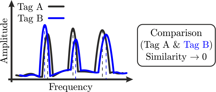
Authentication
Considering the authentication purposes, the information can not be easily replicated by
. Then, even if a counterfeiter knows the object and can copy identically the geometrical characteristics,
the authentication system should be able to differentiate a genuine object. In this
context, chipless authentication relates mainly to guaranteeing the backscattered
signal's uniqueness.
The authentication process is naturally more expensive to implement than
identification since the cost involved in the dedicated test bench and repeated
measurements increase the final solution cost.
Instead of identifying a group of products for the identification purposes, the
chipless authentication focuses on ensuring the received backscattered response in a limited range of products.
The costs involved in ensuring the genuineness of an object are higher than
identification purposes.
The authentication is focused on the differentiation between the signals; it is
highlighted by a coefficient that indicates their similarity level, as depicted in
Fig. 2. The single EM attributes lead to a unique
and unfalsifiable tag-backscattered response. Note that these changes must come only
from the tag signal since any external contribution can yield wrong authenticity
results. Therefore, the contributions other than to the tag, like due to the test bench,
must be suppressed as much as possible. In the identification case, these changes have a
limited effect being absorbed into the definition of frequency windows that attempt to
decode the information.
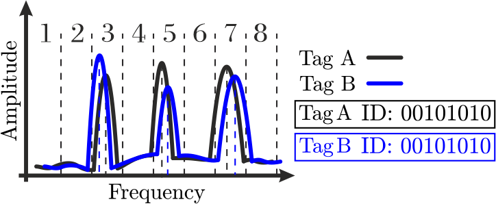
Identification
Identification, in the context of chipless RFID tags, concerns basically encoding a
given information in tag geometry. In this
case, the information can be easily copied by reproducing the tag design. For
example,
if someone copies metallic patterns and reproduces the tag on another product, the
second product will have the ID of the first one. Indeed, chipless
RFID identification relates to identifying the information
impinged in the backscattered spectrum signal (amplitude, phase, time, polarization,
position, or some combination). Therefore, the same ID is recovered despite
the clear difference between the resonance frequencies as shown in
Fig. 3.
Sensor
Besides the authentication and identification functionality, chipless RFID tags can incorporate physical parameters monitoring. Chipless RF sensors can also provide data environments such as temperature, relative humidity, pressure, permittivity, crack detection, moisture, metal dilation, displacement, and location. This information is extracted from the backscattered tag signal. The main task related to chipless RF sensors concerns the isolation of tag signals from surrounding objects/environments.
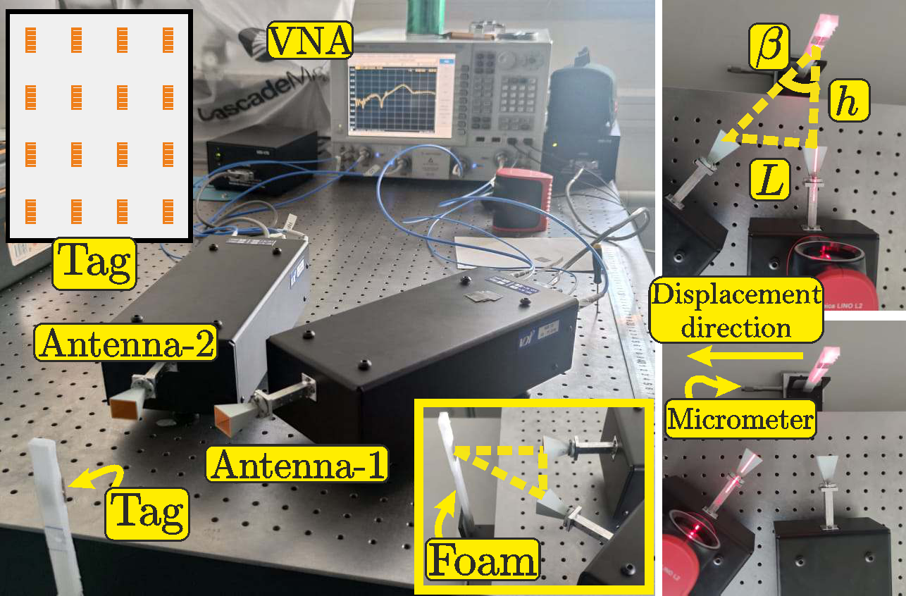
In [2] a displacement sensor based on phase measurement that provides a sub-millimeter positioning accuracy for millimeter wave chipless RFID tag in an office environment. The feasibility of a displacement sensor in which the position is evaluated considering the tag resonance frequency in a bistatic configuration. Furthermore, practical implementation issues considering the bistatic configuration are assessed. The scatterer used for the design of this paper is an E-shape tag [3]. It is a single-layer structure, potentially compatible with a low-cost printing process.
The measurements were performed with an Agilent N5222A $(0.01~\mathrm{GHz} - 26.5~\mathrm{GHz})$ PNA with Virginia Extensions (VDI modules) to operate from $65~\mathrm{GHz}$ to $72~\mathrm{GHz}$ and a power of $0~\mathrm{dBm}$. The VDI module is a frequency multiplier combined with a mixer with a WR15 wave-guide output connected to horn antennas on a co-polarization configuration with a gain of $10~\mathrm{dBi}$. The measurement setup can be seen in Fig. 4. The tag is placed on foam support. The tag is positioned in a different $x$ position for each measurement, and the complex backscatter signal for each tag position is enrolled. The tag has been moved with the help of a micrometer with a step of $30~\mathrm{cm}$ along a constant $h$ position. The distance between the antennas $L = 8.5~\mathrm{cm}$ and the distance to tag plan $h = 13.3~\mathrm{cm}$ are established. Considering all the points over the calculated displacement, an error around $5~\mu\mathrm{m}$ is highlighted. It is a promising result when the results are compared to other chipless tag sensor applications.
Ongoing projects
Morphogenetic generation of electromagnetic components
This research project (ANR-21-CE42-0005) under coordination of Thomas FROMENTEZE focuses on the development of a technique for the bio-inspired procedural generation of electromagnetic components, which enables the automated synthesis of structures. These new microwave components attempt to control/guide the radiated waves to meet electromagnetic radiation requirements. The procedural synthesis of radiating metasurfaces optimized for the realization of multiple polarization-constrained point-to-point links, computational imaging and authentication applications. The versatility of the generative models developed will also enable the procedural synthesis of functionalized materials, suitable for particular for the design of free-form waveguides and generation of anisotropic properties. The activities will be developed in the XLIM laboratory through a combination of simulation and measurement techniques in a wide range of frequencies.
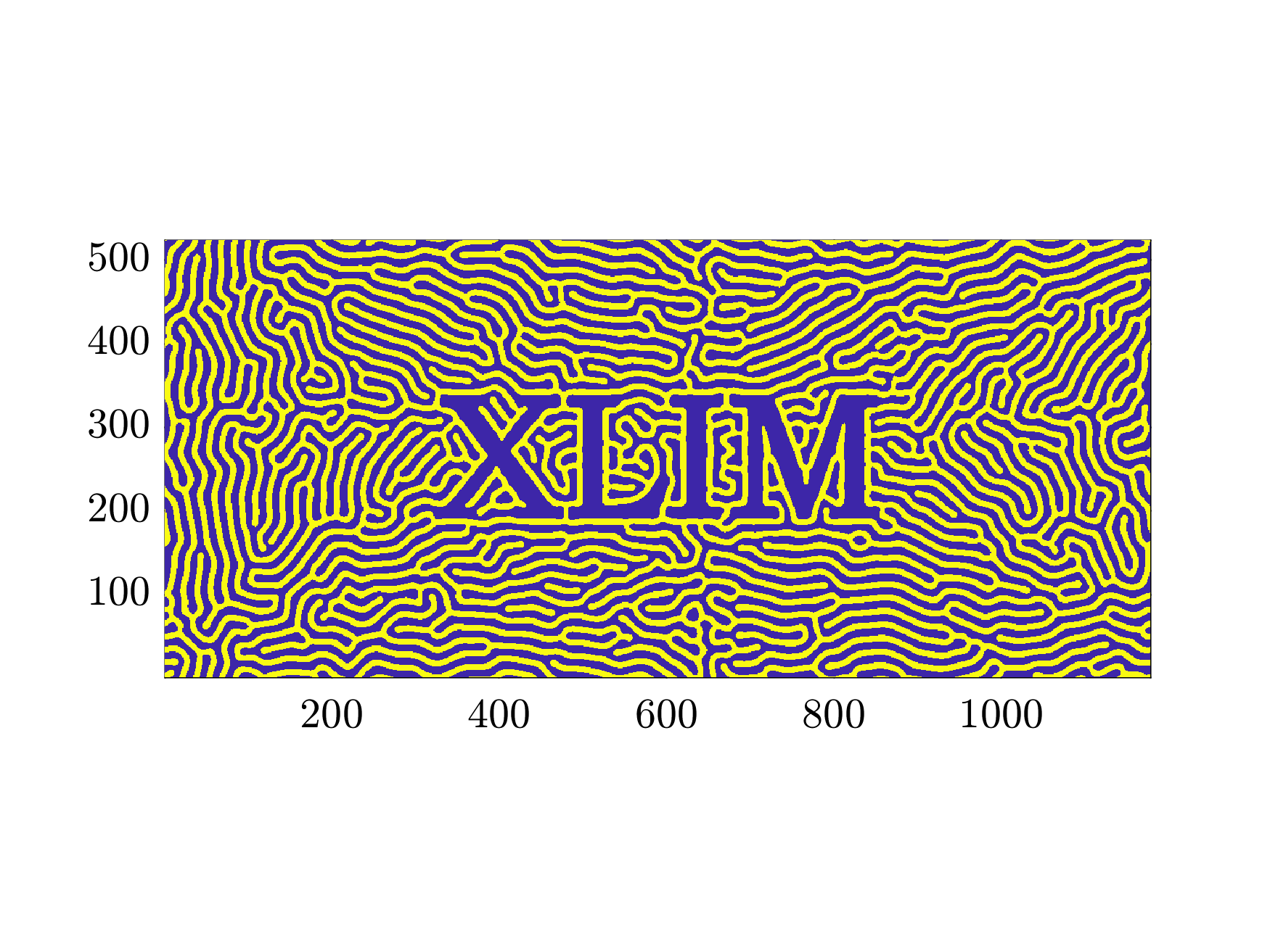
Gray-Scott model
The Gray-Scott model is a simple system of partial differential equations inspired by chemical processes [4]. This reaction-diffusion model involves two species $\mathbf{U}$ and $\mathbf{V}$ which tend to occupy the available space and interact to form spatial patterns when the model is correctly parameterized.
$\begin{eqnarray} \frac{\partial\mathbf{U}}{\partial t} = d_u\nabla^2\mathbf{U}-\mathbf{UV^2}+f(1-\mathbf{U}) \\ \frac{\partial\mathbf{V}}{\partial t} = d_v\nabla^2\mathbf{V}+\mathbf{UV^2} - (f+k)\mathbf{V}\end{eqnarray}$
An example of the generation based on these two equations is shown in the Fig. 5. A self-organized pattern grows to respect a constrained region depicted by the word XLIM.
This model can create spatial distributions of patterns influencing the statistics of induced currents on the generated surfaces. By changing only the initialization of the $\mathbf{U}$ and $\mathbf{V}$ matrices, the pattern types remain constrained, but their spatial distribution will be completely different. This approach thus provides collections of morphogenetic surfaces with controlled average characteristics. This model may pave the way to the generation of novel electromagnetic devices.
Past projects
Authentification Unitaire Sécurisée dans les domaines THz et RAdiofréquencEs - AUSTRALE
My Ph.D. under main coordination of Etienne PERRET and co-coordination of Nicolas BARBOT and Romain SIRAGUSA, was proposed in the context of AUSTRALE (ANR-18-CE39-0002) project, the AUSTRALE project was focused in new low-cost solutions for authentication applications in millimeter-wave and the terahertz (THz) band based on low-cost bio-sourced materials. A consortium of four laboratories worked on the development of new solutions for new authentication systems: the Systems Design and Integration Laboratory (LCIS) for the design of chipless solutions in mmWave, the IMEP-LAHC is charged to develop chipless solutions in THz, the GiPSA that worked on the post-processing aspect and the Technical Paper Center CTP provides low-cost printing solutions.
Counterfeiting, and more generally identity fraud, is a phenomenon that affects all sectors of activity, from luxury goods to mass retailing, and which causes colossal damage in terms of the economy, jobs, brand image and health and technological risks associated with these counterfeit products. In this context, the AUSTRALE project's ambition is to offer new solutions for authentication applications using two major frequency ranges: millimeter waves (MW) and Terahertz (THz). These solutions will be low-cost, compatible with paper industry techniques for mass production, biosourced and easily recyclable. The bio-sourced materials' authentication aspect is evaluated in the context of the AUSTRALE project.
One of the goals of the project is to design and implement a chipless RFID solution to ensure object traceability that presents a unique and unfalsifiable fingerprint obtained from EM signatures. As electromagnetic characteristics are employed, these characteristics cannot be easily spoofed compared to other solutions. Chipless RFID technology authentication provides a non-invasive method based on electromagnetic signature distinction, which does not need a line of sight and is fully printable in bio-sourced materials by low-cost methods. Furthermore, chipless RFID tags can provide a unique and unfalsifiable electromagnetic signature enhancing and assuring their identification. In this context, the contrast between low-cost applications maintaining flexible and trustworthy solutions pave the way for new solutions based on machine learning, radar channel improvement and imaging systems. Different authentication systems are proposed considering chipless tags, and the tag's aspect-independent parameters are evaluated to enhance the characteristics of EM signal uniqueness.
Up to now these original contributions were produced during this project:
- Optimal Angle in Bistatic Measurement for Chipless Tag Detection Improvement
- Millimeter wave chipless RFID authentication based on spatial diversity and 2-D classification approach
- A new method of secure authentication based on electromagnetic signatures of chipless RFID tags and machine learning approaches
- Bistatic Configuration Reading for Sub-Millimeter Displacement Chipless Tag Sensor
- Millimeter-wave Chipless RFID Tag for Authentication Applications
- Design and Manufacture of Resonant Chipless Tags in Millimeter-Wave Band
- Diversité spatiale pour l'augmentation de la robustesse de détection des tags RFID sans puce
Real-time object detection with passive millimeter wave imaging system (mmWave-RTdetect)
Millimeter-wave (mmWave) imaging is widely used for personnel security (e.g. screening at airports, and checkpoints), medical diagnostic image (e.g. cancer diagnosis, vital signs monitoring), military area (e.g. surveillance, reconnaissance), automotive industry (e.g. car movement and pedestrian monitoring) and other fields. Electromagnetic imaging enables the construction of images by the radiated- or scattered-field estimation of a target. In particular, mm-wave imaging provides a fair trade-off between penetration capabilities and resolution, for non-destructive evaluation. Then, mmW radars enable the higher capability to distinguish different targets (resolution) when compared to lower frequency-based devices. Consequently, this technology has undergone an expansion in the last few years and has become competitive in terms of cost. However, a common problem with mmW imaging is the characterization of a field-of-view (FoV), in which the object interacts with the reader. The most of time no interaction between the reader and the object is traduced by no cooperative measurement to image formation.
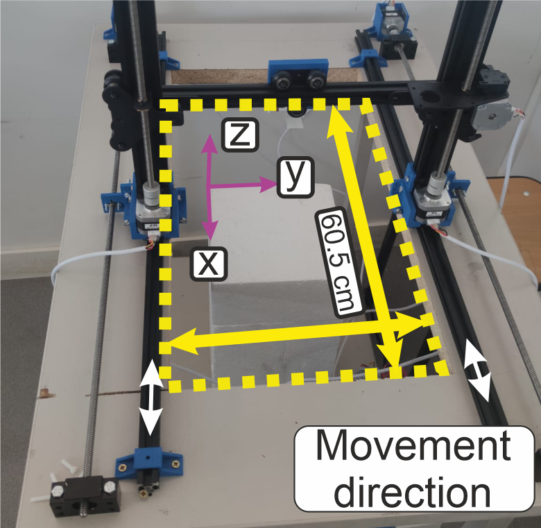
The first objective of the project is to develop a Graphic User Interface (GUI) to
control a 3D displacement table and a
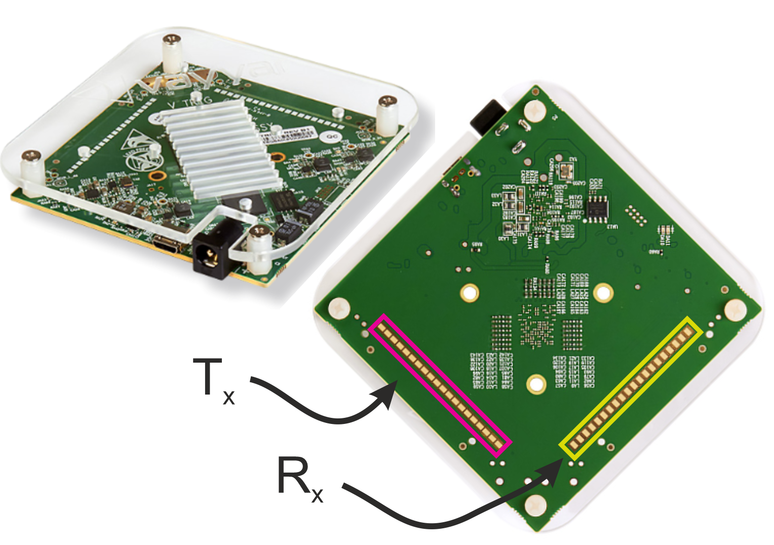
mmW radar (VTRIG-74). The 3D
table and the reader used in the measurements are shown in Fig.
6. Then
the 3D zone in which the radar is able to interact will be characterized. Finally, one
and two
dimensional (2D) effective apertures for resonant (chipless tags) and non-resonant
(metal plate) objects will be done to
validate the measurement bench.
Chipless RFID system application
The main project's objective is the study and integration of a chipless RFID system into a company's extensive range of products for digital product identification methods. In this application, a comprehensive assessment covers all integral components of the system, including the reader, tag, and product. This evaluation ensures a thorough understanding and optimization of the entire chipless RFID ecosystem within company products. The first step relies on understanding and measuring the electromagnetic properties of the range of products. After, some canonical tags are optimized to operate over the range of products. Then, a low-cost specific reader was used to measure the tags.
Dielectric material characterization
The reliability of most components for RF applications is highly dependent on
dielectric material performance. The dielectric characterization at the whole operation
band of the chipless RFID system is essential to assess the system's performance.
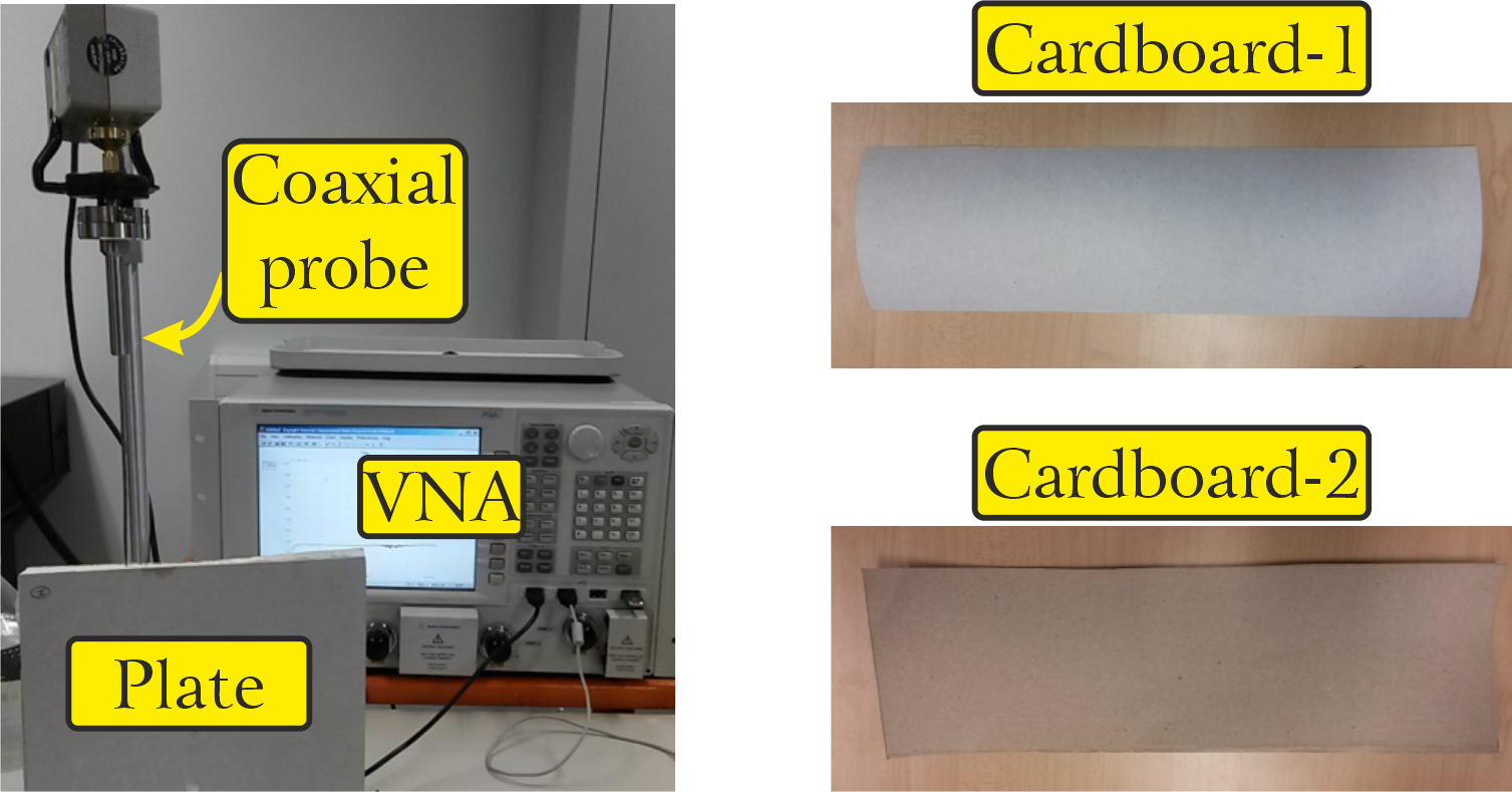
Therefore, the dielectric losses and permittivity are evaluated. For these measurements,
we use two methods, the resonant cavity method and the coaxial probe method for
the characterization of two different materials. The sample consists of a ceramic-type
material (thickness of a few centimeters) covered on each side by a thin cardboard
material (less than one millimeter). First, the cardboard is evaluated in a resonant
cavity. Thus, the plate material is evaluated with a coaxial probe. The plates and
cardboard
material are shown in Fig. 7.
Tag performance under real reading situations
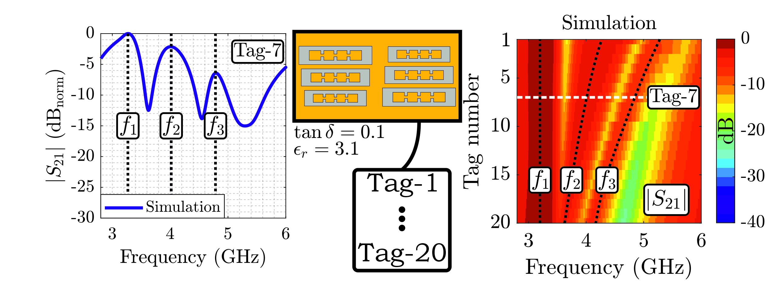
The design, manufacture and test of resonant chipless tags for a commercial application considering their fabrication constraints, losses and the backscattered level are evaluated. A chipless RFID tag solution is developed to operate to overcome the main constraints faced in chipless systems for identification application purposes. A tag inspired on a canonical design barcode and the UHF-RFID [5] was simulated, fabricated and measured. The reading robustness of tag detection was privileged in this designed tag, this tag was built on a paper substrate, as seen in Fig. 8, with loss tangent $(\tan\delta=0.1)$ and relative permittivity $(\epsilon_r = 3.1)$. Due to the losses, three resonators are duplicated aiming to increase the RCS level, making it easier to read and less affected by the clutter. For the measurements, a set of twenty tags with three resonators (3-elements) was fabricated, a co-polarization mono-static configuration was used, and a distance tag-to-antenna of $20~\mathrm{cm}$ was adopted. Each pair of resonators produce $f_1,f_2$ and $f_3$. As depicted in Fig. 8, the first resonance frequency $(f_1)$ is kept fixed, i.e. this frequency serves as a reference. Then, the frequency difference between the first and the other resonances is measured, and according to these differences, a code is established.
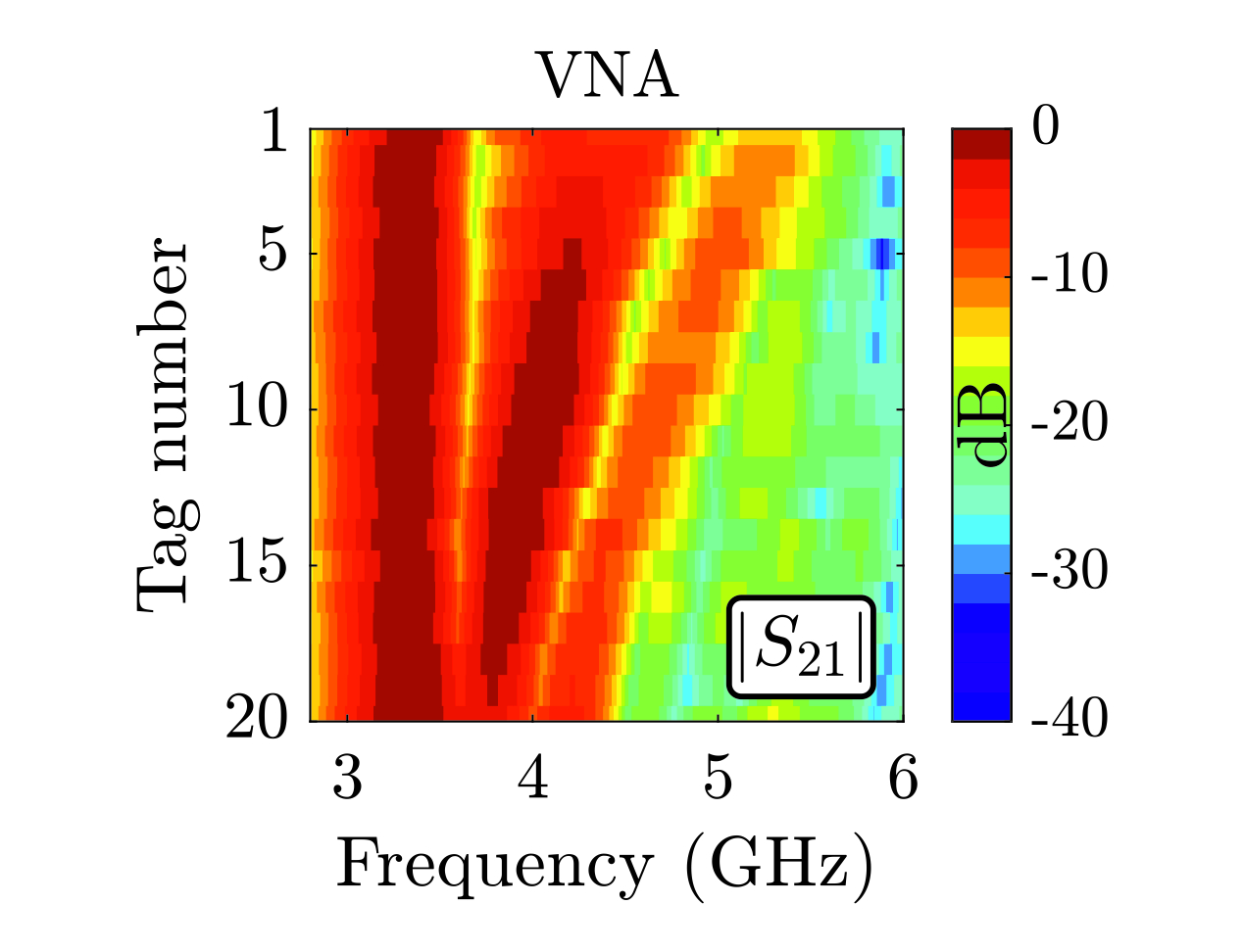
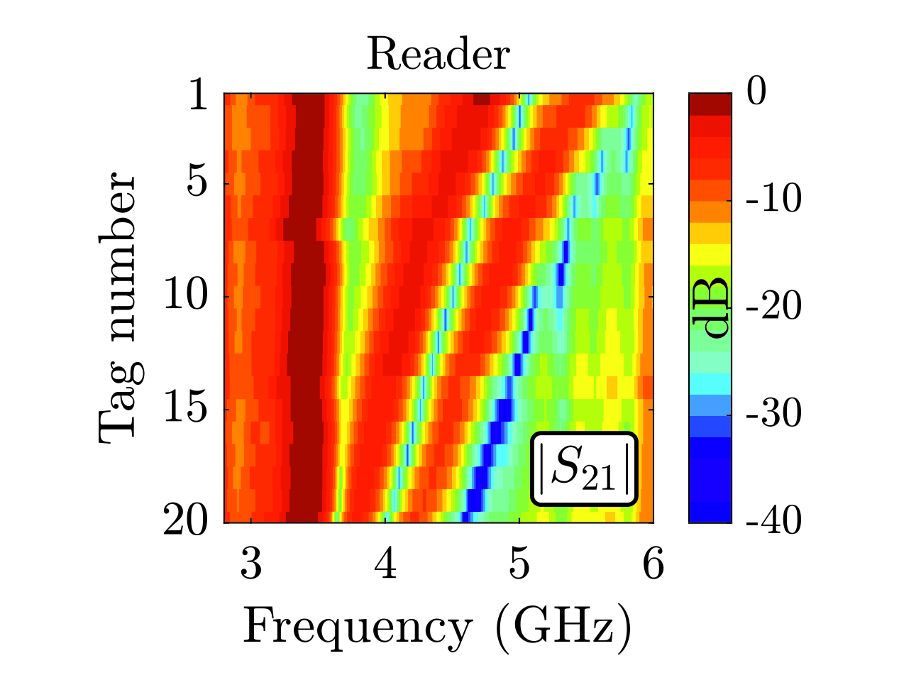
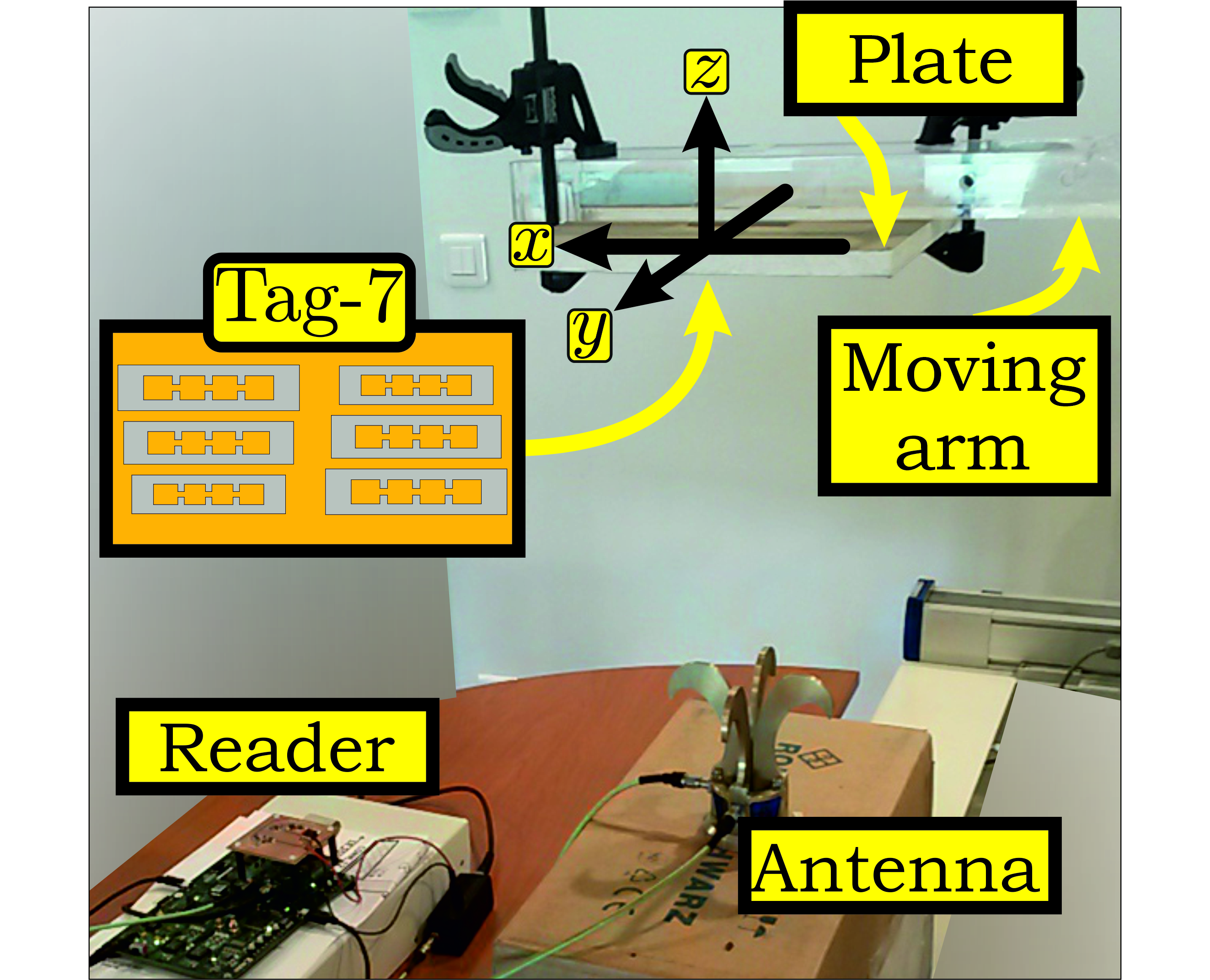
The measurements are evaluated in an office environment with VNA and the reader as shown in Fig. 9. The tag is placed on the plate provided by the company. The and mono-static configurations are performed, the reflection coefficient $(S_{11})$ is measured with one Vivaldi antenna in a co-polarization configuration. A low-cost reader based on impulse-radio ultrawideband (IR-UWB) technology is used for this application [6]. The reader is compliant with the European and American power constraints, designed with equivalent time concept. In the equivalent time concept, the reader continuously sends the same signal. Finally, all samples are recombined by the post-processing step, the backscattered signal is reconstructed.
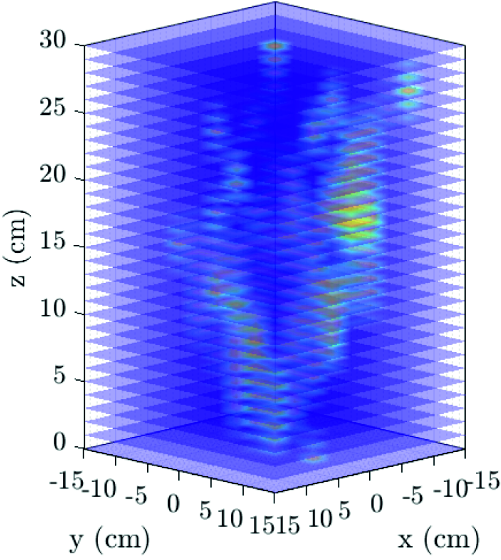
Decoding performance over a 3D characterization zone
A 3D reading region characterization was analyzed, and the reader was used for these measurements. The measurement setup is depicted in Fig. 10(a), a 3-element tag was placed on the plate and the $S_{11}$ was measured and a movement is performed along a 3D zone. A volume of $30~\mathrm{cm} \times 30~\mathrm{cm} \times 30~\mathrm{cm}$ was defined with steps of $0.3~\mathrm{cm}$ for the $x$- and $y$-axis, and for the $z$-axis $1~\mathrm{cm}$ steps were fixed, thus $10000$ positions were analyzed. The 3D table moves along $(x,y,z)$ positions, then the measurement is performed and the $S_{11}$ is stored. After, based on the tag backscattered response, an identifier is attributed to the tag.
In Fig. Fig. 10(b), each color represents that the tag was successfully identified, i.e. the three resonators were compared with one previously established database and the tag was recognized.
As we can see in Fig. Fig. 10(b), on the near antenna region there are many incorrect readings, due to the radiation pattern antenna, then the tag measurements $15~\mathrm{cm}$ away from the antenna are noted that the reading capacity is increased. Since the tag is far away from the antenna, the power level received is lower, so a smaller number of measurements are expected. Therefore, the ideal reading volume with the equipment used is between $20~\mathrm{cm} \times 15~\mathrm{cm} \times 17~\mathrm{cm}$ from the origin. If antennas with different radiation patterns are replaced, the reading range may benefit from longer or closer distances from the antenna.
Low cost UHF-RFID reader
The main objective objective of this project was centered on implementing a UHF-RFID reader using cost-effective components. This project was a joint effort between Me, Carlos Reverbel, and Caroline Gaillard under supervision of Etienne PERRET and of Nicolas BARBOT. Our efforts were focused on designing a UHF-RFID reader system that met EPC standards constraints while using low-cost components.
Communication
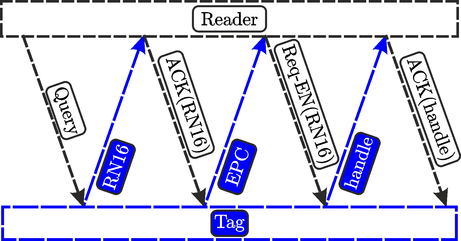
The Electronic Product Code (EPC) protocol defines the physical and logical requirements for a passive-backscatter radio-frequency identification (RFID) system operating in the $860~\mathrm{MHz} - 960~\mathrm{MHz}$ frequency range. The system comprises readers and tags, the communication link between the reader and the tag is half-duplex mode as shown in Fig. 11.
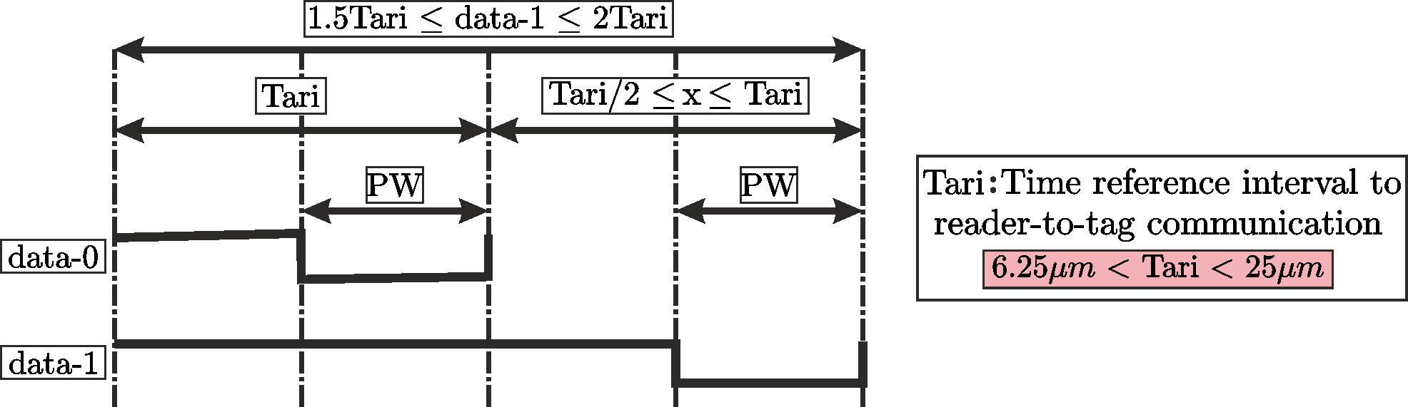
The reader receives and transmits an unmodulated RF carrier and listens for a tag-backscattered reply. Then, the tag replies with a backscatter RF modulation signal. The reader sends information to one or more tags by modulating an RF carrier using a pulse-interval encoding (PIE) format. The PIE is depicted in Fig. 12.
After the definition of data-0 and data-1, the communication protocol to get the tag information is shown in Fig. 13.
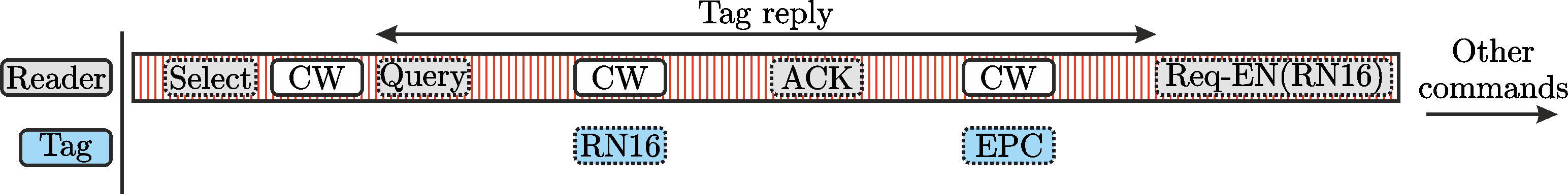
The measurement of the communication between the reader and tag is shown in Fig. 14. In this example, the reader powers up and transmits a Query message that specifies four slots in the frame. The first slot immediately follows the Query command. The second reader command is a QueryRepeat which indicates the beginning of a new slot. In this case, the tag had chosen the second slot to transmit its RN16 in response to the QueryRepeat. Then, it is ACKed by the reader, and transmits its ID. The reader specified four slots in the Query, thus the reader sends two additional QueryRepeats looking for any remaining tags. In this case, there is only a single tag, hence the two slots are empty. In practice, readers perform a series of Query rounds while varying the number of slots based on the number of responding tags. Finally, the tags stop responding once they transmit their ID. This framework is repeated until no tags respond.
